
3D NAND is tough to manufacture. But when it comes to balancing density, durability, and speed at low cost, 3D NAND has changed the game.
The modern data center depends on a vast and intricate network of interconnected technologies, all in service of the chips and drives which directly manipulate and store the data.
Often the same underlying chip technology can be used for different purposes: as storage, as memory, as a microcontroller, etc. But behind multi-purpose chip technologies lie simple truths: chips should be dense, durable, fast, and available at a price reasonable for its use case. When it comes to tech which balances these needs, 3D NAND flash has become the central player.
However, 3D NAND has its own challenges. Firstly, it’s costly and difficult to set up 3D NAND fabs. Another layer of complication is the rapidly changing geopolitical environment, with nations competing to take the lead in chip tech. For example, the U.S. is trying to ramp up domestic chip production, while restricting sales of manufacturing equipment to China.
Even while facing these challenges, 3D NAND is starting to dominate. To name a few examples, it is essential to VAST Data’s all-flash data centers, to WD’s latest hard drives, and to the bread and butter memory and storage functions of enterprises, hyperscalers, and laboratories the world over. 3D NAND will only become more essential as prices fall, and as suitable use cases become more strategically important.
Despite a rocky few years of shutdowns and shortages, chip designers have no shortage of ambition, as they race to add more layers of cells and ramp up density. But no firm is immune to unexpected setbacks. What emerges is a picture of an industry which is ascendent, even though each individual player is precarious.
In other words, the NAND industry is more than the sum of its parts.
The Lay of the Land: Storage and Memory
Computers are more than devices: they’re a paradigm. From pocket devices to hyperscale data centers, everything revolves around the everpresent triangle of storage, processors, and memory.
All computers manipulate data, and that data has to be stored somewhere. For storage, you need non-volatile memory, in which data is retained even after the device powers down. Examples include HDDs, SSDs, and magnetic tape.
You then need to put stored data to work. The main workhorse which fetches and manipulates data is the CPU.
Finally, you’ve got memory, where bits of data can be stored temporarily while the CPU is manipulating other bits. RAM and DRAM are both examples of volatile memory, and don’t retain data when powered down. Non-volatile tech like 3D NAND can also be used as memory.

To sum up, computation requires a CPU, memory, and storage. Storage must be non-volatile, while memory can be volatile, as in RAM.
Flash & 3D NAND
Flash is a type of non-volatile memory. It can be used as storage, as in SSDs, or it can serve as memory proper, subbing in for the more usual DRAM.
Flash comes in two main varieties. NAND flash is slower and less durable than NOR flash, but far cheaper. NAND flash has changed a lot since its early 80s arrival. Most obviously, over time transistors have become progressively smaller, and circuits denser.
Beyond that, one can pack more bits into individual cells. Flash with multi-bit cells (MLC flash) has lower cost-per-terabyte than flash with single-bit cells. However, there’s a catch: MLC flash is denser and cheaper only at the expense of endurance and speed.
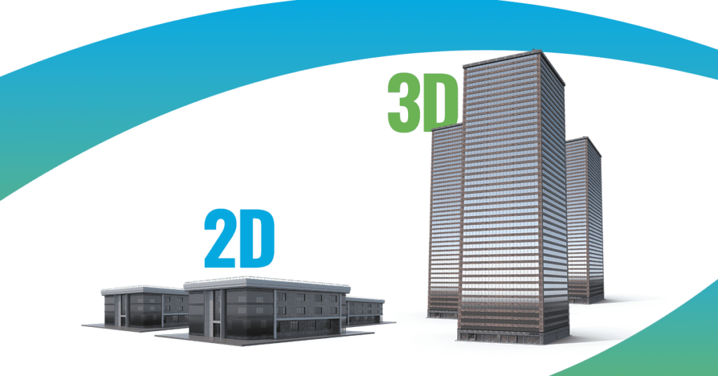
Enter 3D NAND. By stacking cells vertically to the plane of the chip, 3D NAND allows dense storage at lower cost-per-gb, all without sacrificing speed and endurance. In other words, these layered chips let you have your cake and eat it too.
The cost-per-gb is less for 3D NAND than it is for MLC flash. Unfortunately, those low costs only kick in once the fab is built. As we’ll see, the difficulty and expense in setting up 3D NAND fabs is part of what makes modern flash production so fraught.

3D NAND flash is more than just dense and fast: it’s also a key player in efforts to make SSD storage more durable.
Mixing and Matching With 3D Tech
There are several different uses for 3D NAND.
Its speed means 3D NAND is useful as memory, especially for demanding tasks such as running multiple virtual machines or engaging in cutting edge scientific computations. It can also be used as storage, as in WD Blue, Western Digital’s series of 3D NAND SATA SSDs.
It’s also possible to tweak 3D NAND tech for additional density. For example, one can combine the stacking of cells in layers with MLC flash, packing in multiple bits per cell for even denser storage. An example of such stacking and packing is Kioxia’s BiCS flash, based on 3D NAND with three bits per cell.
Finally, note that that the 3D technique isn’t limited to NAND flash. Non-volatile memory may receive the 3D treatment, and Samsung is attempting to develop the first 3D DRAM.
Hard To Optane: A Case Study
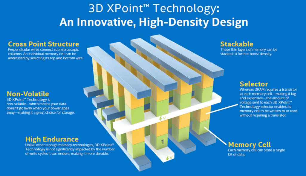
Another example of 3D chip technology is the recently discontinued Optane, co-developed by Intel and Micron. While Optane isn’t a NAND chip, its manufacturing difficulties mirror obstacles to 3D NAND production.
Optane was based on Micron’s 3D X-Point technology. It’s so called because the data access arrays (the silver bars) are at 90 degrees to one another, crossing perpendicularly.
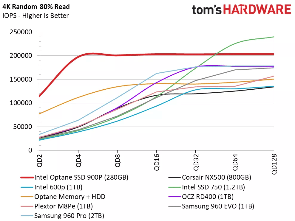
When it came out in 2017, Chris Ramseyer of Tom’s Hardware called Optane 900P a “near mythical creature”. He insisted that “The difference between the Optane 900P and everything that came before it is simply unbelievable”.
The IOPS were particularly impressive, making Optane excellent for low-latency applications.
Fast forward half a decade, and Intel is discontinuing the technology. What gives?
Intel may not have had much of a choice. Recall that Optane was co-developed with Micron. Micron also fabricated the 3D Xpoint chips that figured in Optane. In 2018, Micron pulled out of the partnership, leaving Intel with an Optane surplus, and no easy way to fabricate the needed chips.
Facing a 17% y-o-y decline in revenue in 2Q2022, Intel decided to write the remaining Optane off as a loss.
3D NAND Designers: Trouble in Paradise?
Optane isn’t an isolated incident. We like to think that chip designs rise and fall on their own merits, with the most innovative solutions inevitably rising to the top. But the world is complicated.
As it involves connecting multiple layers with tiny vertical channels, 3D chips are difficult enough to manufacture that the maneuvering of major players is an important factor in the success of a line of chips. Mergers, spinoffs, and internal strife, if not managed carefully, provides drag which can give competitors a crucial opening.
Samsung has lost two of its largest customers to Taiwanese chipmaker TSMC. According to one analyst, a contributing factor is issues with company culture. Meanwhile, WD continues to face pressure from Elliot Management, an activist investor who wants WD to spin off its flash business. Intel has already exited the SSD business, selling its fabs to SK hynix back in 2020.
Kioxia is navigating rocky terrain as well: in a fab co-run with WD, contamination led to a loss of up to 16EB of flash. Also, Toshiba, which is currently facing breakup pressure, holds 40% of Kioxia’s shares
A handfull of dominant players shape 3D NAND production. But that’s not the whole story: within and between these giants, the situation is more fluid than one would expect. Partnerships are made and broken, fabs change hands, and unexpected setbacks give rival companies a chance to pounce.
While it may be a temporary trend, reduced demand has put pressure on chip manufacturers as the pandemic surge in tech spending winds down. Micron is reducing utilization for some NAND fabs, and Kioxia is cutting down production in their Japanese fabs. SK Hynix is reducing investment by more than 50% in the face of reduced demand.
YMTC and Geopolitics
Enter YMTC. The Chinese chip manufacturer receives heavy subsidies, which seem to have paid off.
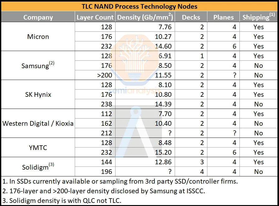
YMTC’s 3D NAND chips are tied with Micron’s at 232 layers, but beat out Micron’s 14.64 G/mm^2 with a denser 15.2 GB/mm^2. That means the Chinese firm makes some of the densest TLC (three bits per cell) 3D NAND in the industry. Add to this its plans for another new fab, and it looked like YMTC was set to become a major player.
Then came the U.S. trade restrictions on production equipment. The stated reason was to make it more difficult for Chinese firms to make chips which could be used in military technology.
The effect of the restrictions was swift. Applied Materials, KLA, and Lam Research, all based in the U.S., have ceased selling 3D NAND with 128+ layers to YMTC. Dutch firm ASML has also ceased shipping equipment to Chinese customers.
Affected tools include ones for etching, inspection, die sorting, and more. This could eventually lead YMTC to reduce or cease 3D NAND production, although supply is currently secure.
Clearly, competition between chip designers isn’t the only engine driving shifts in manufacturing. National rivalries and geopolitical considerations are crucial as well, with several nations vying to increase domestic manufacturing.

A major development in the geopolitics of chip design is the passage of the CHIPS Act in the U.S, which aims to shift the global center of gravity of chip design.
A World of Possibilities
As we’ve seen, 3D NAND is a complex industry. The challenge of fabrication, the ever-shifting business landscape, and the backdrop of geopolitical competition mean that designers and manufacturers have a lot on their plate.
At this point it’s worth reminding ourselves why 3D NAND sparks so much competition. Simply put, the upsides, in terms of durability and speed, are worth it. Here are some examples of how innovators have found new ways to put 3D technology to work.
One great use-case of 3D NAND is within all-flash arrays and data centers.
For example, VAST Data offers “Universal Storage”, a single-tier all-flash storage solution. They previously used Intel’s 3D QLC NVMe flash in its arrays together with 3D X-point technology (Optane) to store metadata. Now that Optane has been discontinued, VAST stores metadata with a chip that incorporates Kioxia’s 3D NAND BiCS technology.
Other players pushing all-flash solutions include PureStorage, Dell, and NetApp. PureStorage also uses 3D NAND in its arrays, as does Dell.
Western Digital has found a totally different use for 3D NAND. It outfitted its HDDs with “OptiNAND” technology, which stores metadata, freeing up more space on the disk for proper storage.
OptiNAND is based on WD’s iNAND technology, which outfits its 3D NAND flash with a special controller. Just because 3D NAND is great for all-flash arrays doesn’t mean it can’t get along with its older relatives.
3D Players Add More Layers
The benefits of 3D NAND are clear. Companies know this, and are working hard on ever denser flash storage.
Samsung has recently launched a 3D NAND chip boasting record density. The 236-layer chip has a capacity of 1TB, and is currently being mass-produced. The firm’s future plans are even more ambitious, as the firm works on its transition to QLC (four bits per cell) 3D NAND. By 2030, Samsung hopes to have 1000+ layer NAND. This could put a 1PB SSD within reach.
Solidigm is also pursuing QLC, and plans to incorporate it into a 61TB 3D NAND chip with 192 layers, which would beat out Micron’s 176 layer QLC NAND.
After Samsung, Micron currently produces the second-densest 3D NAND, a TLC chip with 232 layers. The chipmaker hopes to eventually work its way up to a 500-layer NAND chip.
Since the technique of packing multi-bit cells can be combined with 3D NAND, this means that designers trying to increase chip density need to choose between packing and stacking. For instance, one SK hynix chip has a stunning 238 layers, but is far from the densest chip around, as it only packs in three bits per cell.
Innovations in 3D NAND Design
Is there a limit to how many layers you can stick in a 3D NAND chip? Yes.
To connect layers in 3D NAND chips, manufacturers must etch wafers with tiny holes. These have a high-aspect ratio: a hole a few micrometers deep will still have a diameter of only 120 nanometers. And of course the more layers a chip has, the deeper these holes need to be.
“There are advances in the etch technology to etch deeper holes in one go, but it won’t go faster. You can’t increase the speed of the etch. So if the process flow get dominated by the deposition and etch, and those process steps don’t increase in cost efficiency, then adding more layers is not as efficient anymore to reduce the cost.”
Maarten Rosmeulen, Program Director at Imec.
Another complication is that these tiny holes need to be filled with a thin dielectric layer, which is a challenge. Also, warping also becomes more likely as the layers stack higher.
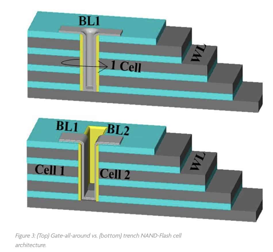
One solution to increase density in 3D NAND chips is “trench architecture”. Instead of drilling a cylindrical hole and coating it all the way around with dielectric material, you coat either side of the hole separately, leading to two cells rather than one.
Another density workaround is “4D NAND”, developed by SK Hynix. This is a variant of 3D NAND that uses “PUC”, for “periphery under device”. Basically, this frees up space by tucking peripheral circuits beneath, rather than in between, cells.
A Many Layered Industry
The 3D NAND industry is unique: the whole is greater than the sum of its parts.
On the one hand, 3D NAND is a revolutionary technology. It has achieved a better balance between density, speed, durability, and cost-per-gb than any other flash.
On the other hand, no one player in the market is full-proof. Cutting-edge 3D tech like Optane can vanish overnight, and trouble in a fab can set a company back a long time.
Despite all the struggles of individual players, 3D NAND is in a good spot. In fact, a recent report says that the 3D NAND market is set to grow between 22-25% CAGR.
The precarity may be good for development in the end: in such a rapidly evolving landscape, each company has the possibility of taking the lead.
Chips may start out in labs and fabs, but it’s your company that decides where they ends up. Horizon Technology can help you reduce e-waste and properly reuse and recycle decommissioned tech.